The semiconductor industry is booming, but the environmental toll of its manufacturing waste is hard to ignore. From fabrication to global shipping, the sector leaves a significant carbon footprint. Packaging, once a side note, has now taken center stage for companies determined to lower their emissions and operate more sustainably.
Traditional semiconductor packaging is wasteful and carbon-heavy. To address this, leading companies like TSMC, Samsung, and Intel are rapidly securing intellectual property (IP) for low-carbon, reusable, and biodegradable solutions, aiming to revolutionize logistics while maintaining product integrity.
Innovations in eco-friendly semiconductor packaging
IP is driving real change in how the semiconductor industry approaches packaging. Significant advances are evident in:
- Biodegradable materials: Plant-based plastics and recyclable composites are now viable, cutting waste while maintaining product safety.
- Reusable packaging: Patent-driven modular solutions are making it possible to reuse casings, which significantly reduces single-use plastics.
- Lightweight packaging: Optimized materials keep shipping costs and emissions down across global supply chains.
- Smart packaging: Advanced tracking and climate-adaptive features are improving security and reducing environmental impact.
Role of IP
Companies are aggressively patenting innovative solutions, such as self-repairing materials, carbon-neutral shipping processes, and advanced nano-technology. Furthermore, industry leaders are licensing these technologies, which speeds up industry-wide adoption and ensures sustained capital flow and operational momentum.
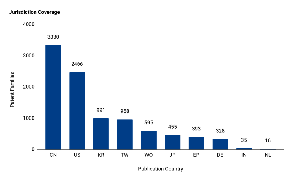
Competitiveness today is closely linked to innovation in sectors like carbon-capture packaging, smart logistics, and flexible architectures. Given the speed of technological advancement, staying ahead requires moving beyond traditional solutions.MaxVal’s IP analysis in this space revealed that China’s activity is particularly noteworthy. Recent filing trends reveal a massive consolidation of IP assets within the advanced packaging sector, a move clearly aimed at maximizing manufacturing resilience and bypassing traditional scaling limitations. For companies reliant on semiconductors, understanding this shift is crucial, as it is likely to shape future industry standards. A glimpse into jurisdiction trends and top global filers from our study is provided below:
Jurisdiction Coverage (2020-25)
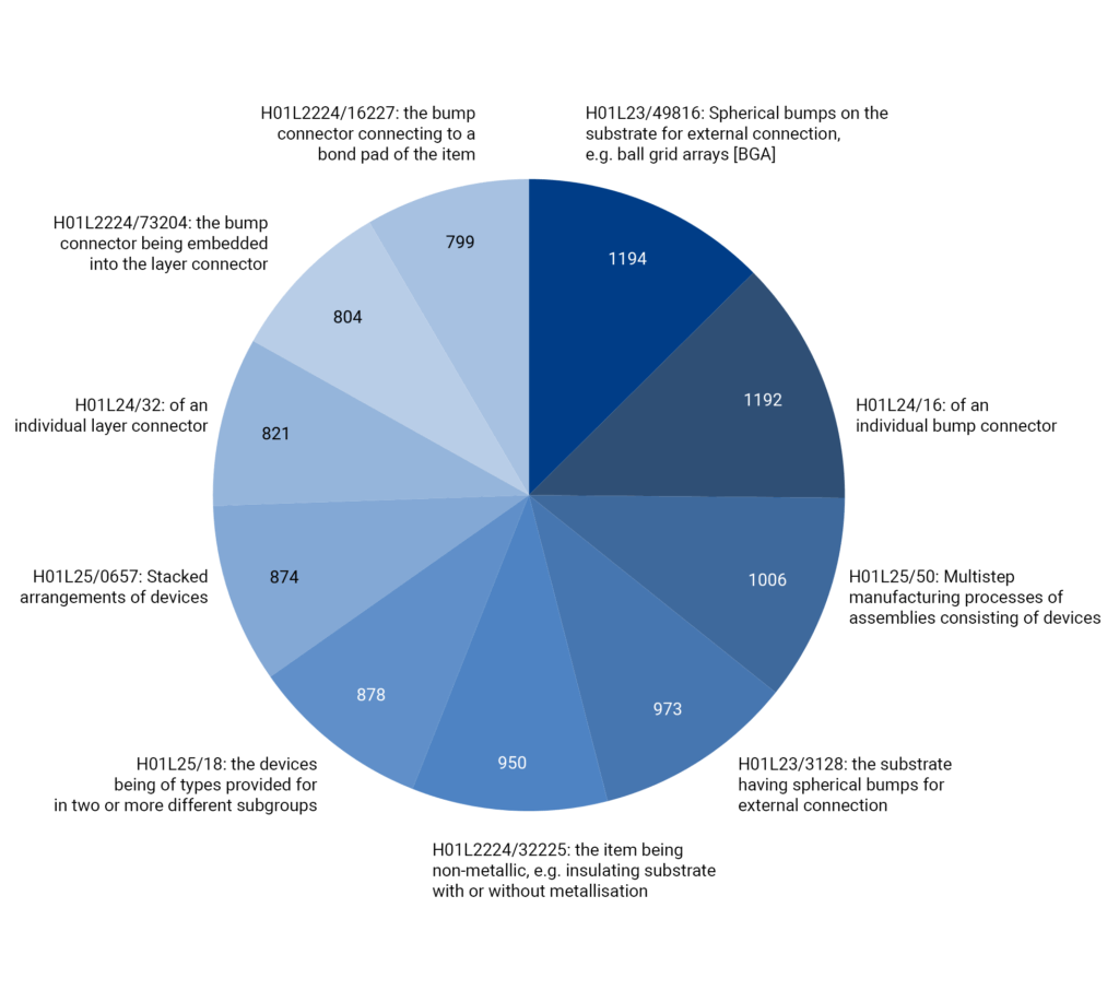
Top CPCs:
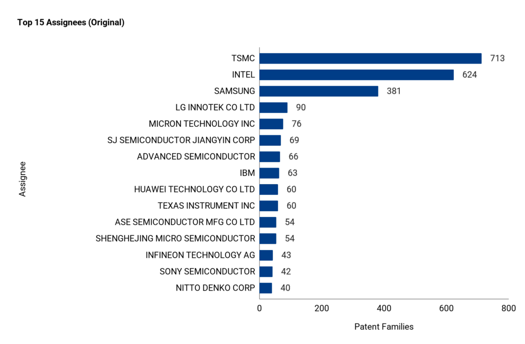
Top Assignees (2020-25)
A major manufacturing alliance between TSMC, Amkor, and Apple was formed in 2024, targeting carbon-neutral silicon by 2030 and already deploying biodegradable, ultra-light packaging to cut down on shipping emissions. It is a full-stack approach to sustainability and is quickly becoming the norm.
Some innovative patents by top industry leaders who are driving these changes with innovative solutions are provided in the following table:
Semiconductor Packaging Sustainability Innovations
| Company | Patent Number(s) | Key Innovation | Sustainability Impact |
|---|---|---|---|
| TSMC |
US20240363559A1 US20240371803A1 |
Compact packaging & Carbon-free etchant for RDL | Reduces hazardous waste and transport emissions. |
| US20240213213A1 | Resin-based stress absorbers | Lowers encapsulant volume and improves yield. | |
| Samsung | US20240145396A1 | Bio-polymer molding & biodegradable carrier film | Introduces plant-based materials to high-tech FOWLP. |
| Micron | US20250046723A1 | Decomposable interfaces & biodegradable polymers | Allows for end-of-life degradation, cutting e-waste. |
| Infineon | US20250096056A1 | Porous inorganic colorant in matrix material | Minimizes raw material consumption. |
| US20230420319A1 | Metal-activated inorganic filler particles | Extends package life, reducing replacement frequency. | |
| KLA Corp | US11036898B2 | Reusable substructure for nanowires | Enables modular reuse instead of single-use inserts. |
The next frontier: unexplored IP in eco-friendly semiconductor packaging
Our detailed analysis revealed some unexplored technology spaces offering significant scope for research:
- Self-Healing Packaging Materials: Development of materials that can repair micro-cracks, extending packaging lifespan, and reducing waste. For example, CN108440740B (Suzhou University) discloses a self-healing epoxy resin for semiconductor packages using reversible cross-link chemistry.
- Bio-Based Conductive Packaging: A focus on conductive organic materials to replace traditional metallic shielding while being eco-friendly. CN115651167A (Xi’an Jiaotong University) reports a biodegradable, plant-based epoxy-cured material tailored for IC packaging that degrades in industrial composting.
Strategic IP considerations
Navigating the sustainable packaging landscape requires a sophisticated IP strategy beyond simple filing. As the sector matures, companies must consider:
- Strategic Defensive Filings: In fast-moving sectors such as bioplastics, the goal of patenting often shifts from exclusivity to protection. A defensive IP strategy ensures a company retains the right to innovate without being blocked by competitor filings, effectively “staking a claim” to future technological territory.
- Freedom-to-Operate (FTO): With global players like Samsung and TSMC aggressively filing, conducting thorough FTO searches is critical to ensure new biodegradable solution(s) don’t infringe on existing rights.
- IP Monetization & Partnerships: Eco-friendly technologies offer significant value beyond direct manufacturing. Organizations can leverage their green IP portfolios through licensing agreements with major foundries, transforming R&D breakthroughs into lucrative revenue streams while establishing market leadership.
Conclusion
Sustainability has evolved from a regulatory requirement into a core competitive strategy for the semiconductor industry. As global standards tighten, the companies that will lead the future of logistics are those that successfully integrate scalable, carbon-neutral packaging with a robust IP portfolio. Securing patents in this space is no longer just advantageous; it is the deciding factor in determining which organizations will dominate the next era of manufacturing. However, winning this race requires navigating an increasingly complex and crowded IP landscape where standard data is not enough. MaxVal empowers R&D and IP teams with actionable intelligence, helping them master the intersection of advanced materials and manufacturing logistics. By providing precise insights on where to innovate, file, and license, we ensure your organization makes the informed decisions necessary to secure a sustainable and competitive future.